In the world of electronic devices, printed circuit boards (PCBs) and PCBA are the backbone of every functioning system. One of the fundamental features of PCBs is the presence of through holes, which are essential for the connectivity, stability, and overall performance of the board. While surface mount technology (SMT) has become increasingly popular due to its compactness and efficiency, through-hole technology still plays a vital role in certain PCB designs. In this blog, we’ll explore the importance of through holes in PCB design, their advantages, and the manufacturing processes that make them a key component in electronics.
What Are Through Holes in PCB?
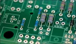
Through holes, also known as plated through holes (PTH), are holes drilled through the entire PCB, from the top layer to the bottom, and sometimes through multiple layers in the case of multi-layered PCBs. These holes are typically lined with copper, which allows for electrical conductivity between different layers of the PCB. Through holes enable the insertion of components with leads that pass through the PCB, and they are secured using solder.
Through holes are generally used for larger components, like connectors, resistors, capacitors, and even some mechanical components, which require a solid mechanical connection to the board.
Why Are Through Holes Important?
- Strong Mechanical Connection
One of the main reasons through holes are still in demand is their ability to provide a strong mechanical connection. Since the leads of the components pass through the PCB and are soldered to the opposite side, the components are more firmly anchored in place compared to surface-mount components, which rely only on the solder to hold them. This makes through holes ideal for applications that experience high mechanical stress, vibrations, or where the components need to be physically secured for durability.
1418. Multi-Layer Connectivity
In multi-layered PCBs, through holes are crucial for creating connections between the different layers. These holes, also known as vias, allow electrical signals to pass from one layer of the PCB to another. By drilling through the PCB and electroplating the holes, manufacturers can ensure that the PCB functions correctly, with components located on different layers being able to communicate electrically. This makes through holes essential for complex circuit designs that require multiple layers to house a high density of components.
1419. Ease of Maintenance and Repair
Through-hole components are easier to repair or replace than surface-mount components. If a component fails, it can be desoldered and replaced without the need for specialized equipment. This makes through holes a better option for designs that need to be serviced or for applications in industries where long-lasting, repairable electronics are critical. In contrast, surface-mounted components often require more intricate and expensive equipment for replacement.
1420. Higher Power Handling
Through holes are often preferred for high-power applications, as they offer a more robust electrical connection. The thicker leads of through-hole components can handle higher currents compared to their surface-mounted counterparts. This is particularly beneficial for power electronics, motor control systems, or any applications that require high power, such as industrial equipment or automotive electronics.
1421. Better Thermal Dissipation
Due to their larger size and robust mounting, through-hole components generally provide better heat dissipation compared to surface-mounted components. This is especially important in power-intensive devices where heat management is crucial to prevent damage to both the components and the PCB itself.
Types of Through Holes
- Standard Through Holes
These are the traditional through holes where the component’s leads pass through the entire PCB. They are the most common type used for large components such as connectors, electrolytic capacitors, and resistors. Standard through holes are typically used for low to medium-density designs.
3875. Blind Vias
Blind vias are through holes that connect the outer layer(s) of a PCB to one or more inner layers, but do not pass all the way through the PCB. These are used to route electrical connections between specific layers of a multi-layer PCB without affecting the outer layers. Blind vias are often found in high-density interconnect (HDI) boards.
3876. Buried Vias
Buried vias are similar to blind vias but are located entirely within the inner layers of the PCB and do not connect to the outer layers. These vias are typically used in multi-layer designs to reduce space and increase routing density, which is particularly beneficial for advanced electronic devices that require compact and high-performance PCBs.
3877. Via-in-Pad
A via-in-pad is a design technique where a through hole is placed in the pad of the component. This is often done to reduce space on high-density boards or to increase the mechanical strength of the pad. However, this design can present challenges during manufacturing and soldering, so it must be carefully considered.
The Manufacturing Process for Through Holes
- Drilling
The process starts with drilling holes in the PCB. These holes are usually drilled with high-precision equipment to ensure that they are of the correct size and location. The drill size depends on the component leads and the desired electrical path.
5332. Copper Plating
After the holes are drilled, they are electroplated with copper. This is done by immersing the PCB in a copper bath and applying an electric current to deposit copper onto the walls of the drilled holes. This copper plating forms the electrical connection between the layers of the PCB.
5333. Soldering
Once the components are inserted through the holes, they are soldered to the PCB, securing the component mechanically and electrically. The soldering process may be done manually or by using wave soldering or reflow soldering methods, depending on the design and the production volume.
5334. Inspection and Testing
After the soldering is complete, the PCB undergoes inspection. Automated optical inspection (AOI), X-ray inspection, and electrical testing are commonly used to ensure the integrity of the through holes, ensuring that they are properly plated, aligned, and free from defects such as solder bridges or misalignments.
Challenges of Using Through Holes
While through holes have their advantages, they come with some challenges:
- Increased Manufacturing Complexity
The process of drilling and plating through holes can add complexity and cost to the manufacturing process. The additional steps and equipment required for through-hole technology can make it more expensive than surface-mount technology, especially for designs that don’t require high durability or mechanical strength.
6692. Size Limitations
Through-hole components generally require more space on the PCB due to their larger size and the need for drilling. This can limit the density of components on the board and may not be suitable for compact or miniaturized devices.
6693. Longer Assembly Times
The process of inserting and soldering through-hole components can be slower compared to surface-mount components, which can be automatically placed and soldered in high-volume production lines.
Conclusion
Through holes continue to be an integral part of PCB design, offering reliable electrical connections, mechanical strength, and ease of maintenance. Despite the rise of surface-mount technology, through-hole components remain essential in many industries, particularly where high-power applications, repairability, and long-term durability are key considerations. By understanding the role of through holes and the manufacturing process involved, engineers can make informed decisions when designing PCBs for various applications, ensuring the best performance and reliability for their electronic devices.